タグ

半導体

27 件の記事

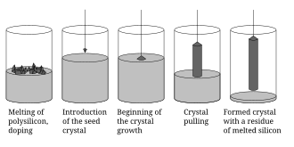
The Czochralski method

ウェハーの基礎知識半導体製造を支える基板の仕組みと進化

ウェハー半導体シリコンウェハーチョクラルスキー法
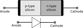
A p–n junction diode. The circuit symbol is also shown.

P-n接合の仕組みと半導体デバイスへの応用

p-n接合半導体ダイオード空乏層
Pourbaix diagram of iron.[6]

不動態化(パッシベーション)の仕組みと産業利用金属の腐食を防ぐ表面処理技術

不動態化パッシベーション表面処理耐食性
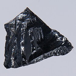
Silicon crystals are the most common semiconducting materials used in microelectronics and photovoltaics.

半導体デバイスの基礎から進化まで材料特性と製造プロセスの全貌

半導体シリコンドーピングトランジスタ
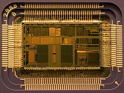
An integrated circuit (IC) as an example application in the field of microelectronics. The chip housing is opened to allow a view of the actual circuit. The golden connecting cables, which form the electrical wiring between the IC and the housing contacts, can be seen on the sides.

マイクロエレクトロニクスの基礎超小型電子回路の仕組みと設計

マイクロエレクトロニクス半導体集積回路IC

Color lines in a spectral range

ハフニウムの特性と産業利用ジルコニウムとの密接な関係と先端技術への応用

ハフニウムHf遷移金属ジルコニウム
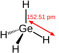
Structural formula of germane

ゲルマン(Germane)の特性と半導体産業における役割

ゲルマンGeH4ゲルマニウム半導体

Color lines in a spectral range

ホウ素(ボロン)の特性と産業・医療への応用

ホウ素ボロン周期表ホウ酸塩
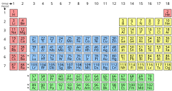
The periodic table.

準金属(メタロイド)の特性と現代社会における役割

準金属メタロイド半導体周期表
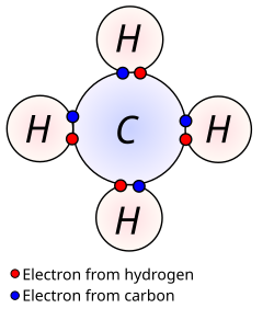
Four covalent bonds. Carbon has four valence electrons and here a valence of four. Each hydrogen atom has one valence electron and is univalent.

価電子の基礎知識化学結合と元素の反応性を決定する仕組み

価電子化学結合電子配置オクテット則

Kyushu from the International Space Station

九州の地理・文化・経済アジアへの玄関口としての魅力

九州地理経済文化
Color lines in a spectral range

シリコン(ケイ素)の特性と現代社会への影響

シリコンケイ素半導体電子デバイス