タグ

ムーアの法則

4 件の記事

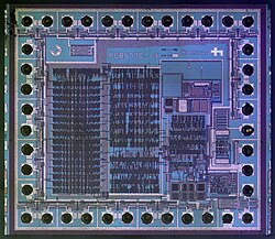
A microscope image of an integrated circuit die used to control LCDs. The pinouts are the dark circles surrounding the integrated circuit.

集積回路(IC)の仕組みと進化現代テクノロジーを支えるマイクロチップの全貌

集積回路ICマイクロチップ半導体
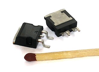
Two power MOSFETs in D2PAK surface-mount packages. Operating as switches, each of these components can sustain a blocking voltage of 120 V in the off state, and can conduct a con­ti­nuous current of 30 A in the on state, dissipating up to about 100 W and controlling a load of over 2000 W. A matchstick is pictured for scale.

MOSFETの仕組みと進化現代エレクトロニクスを支えるスイッチング技術

MOSFET電界効果トランジスタ半導体CMOS
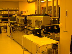
A semiconductor device manufacturing facility at HP Labs

半導体デバイス製造の進化とプロセスノードの真実

半導体製造プロセスノードウェハフォトリソグラフィ
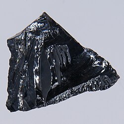
Silicon crystals are the most common semiconducting materials used in microelectronics and photovoltaics.

半導体デバイスの基礎から進化まで材料特性と製造プロセスの全貌

半導体シリコンドーピングトランジスタ