私たちの生活に欠かせないスマートフォンやコンピュータ、家電製品。これらの心臓部で複雑な計算や制御を担っているのが集積回路(IC:Integrated Circuit)です。一般的に「チップ」や「マイクロチップ」と呼ばれるこの小さな部品は、現代社会のデジタル革命を根底から支える基盤技術となっています。
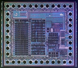
ICとは、トランジスタ、抵抗器、コンデンサといった個別の電子部品とそれらを結ぶ配線を、シリコンなどの薄い半導体基板の上にひとまとめに作り込んだ回路のことです。かつては個別の部品を一つずつ配線して回路を組んでいましたが、ICの登場により、回路の極小化、高速化、そして低コスト化が同時に実現しました。
Key Facts
- 構成要素:シリコンなどの半導体上にトランジスタや抵抗、コンデンサを統合して形成される。
- 主要な利点:個別の部品を組み合わせた回路に比べ、サイズが劇的に小さく、消費電力が低く、処理速度が速い。
- 進化の法則:ムーアの法則に従い、同じ面積に搭載できるトランジスタ数は飛躍的に増加し続けている。
- 汎用性:データ処理、制御、記憶など、あらゆる電子機器の基本機能を提供している。
集積回路の歴史と技術的転換点
黎明期とモノリシックICの誕生
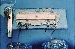
ICの歴史は1960年代に遡ります。世界初の集積回路はジャック・キルビーによって開発され、ゲルマニウム素材と金線を用いた構造でした。その後、1959年にはロバート・ノイスがシリコンを用いた「モノリシック(単一の結晶からなる)」集積回路を発明し、これが現代のIC製造の基礎となりました。

論理回路の発展:TTLからMOSへ
1960年代から80年代初頭にかけては、ジェームズ・L・ビューイが開発したTTL(トランジスタ・トランジスタ・ロジック)がデジタルICの主流でした。しかし、その後、より高密度な実装が可能なMOS(金属酸化物半導体)技術が登場します。
特に1968年にフェデリコ・ファギンが開発した自己整合ゲート付きMOS IC技術は、現代のCMOS(相補型MOS)の基盤となりました。これにより、一つのチップにコンピュータの演算機能をすべて盛り込む「マイクロプロセッサ」や「マイクロコントローラ」の実現が可能になったのです。

ICの構造と製造プロセス
内部構造の階層化
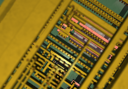
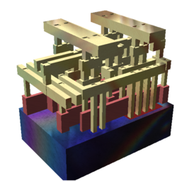
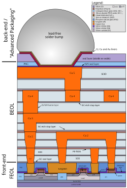
現代のICは、極めて複雑な多層構造をしています。最下層にはシリコン基板があり、その上にポリシリコンのゲートやウェル(不純物領域)が形成されます。さらにその上には、信号を伝達するための銅などの金属配線層が何層にもわたって重ねられています。
製造からパッケージングまで
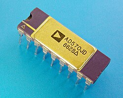
ICの製造は、半導体ウェハー上への微細な回路形成(前工程)と、切り出されたダイ(チップ本体)を外部端子と接続して保護ケースに封入するパッケージング(後工程)に分かれます。パッケージの形態には、DIP(デュアルインラインパッケージ)などの伝統的なものから、BGA(ボールグリッドアレイ)のような高密度なものまで多様に存在します。
集積度の進化:SSIからULSIまで
ICは、一つのチップに搭載される素子の数によって、以下のように世代が分類されます。1960年代の単純な回路から、現代の数十億個のトランジスタを搭載する超大規模集積回路へと進化してきました。
| 略称 | 名称 | 登場年 | トランジスタ数 | 論理ゲート数 |
|---|---|---|---|---|
| SSI | 小規模集積回路 | 1964年 | 1 〜 10 | 1 〜 12 |
| MSI | 中規模集積回路 | 1968年 | 10 〜 500 | 13 〜 99 |
| LSI | 大規模集積回路 | 1971年 | 500 〜 20,000 | 100 〜 9,999 |
| VLSI | 超大規模集積回路 | 1980年 | 20,000 〜 1,000,000 | 10,000 〜 99,999 |
| ULSI | 極大規模集積回路 | 1984年 | 1,000,000以上 | 100,000以上 |
初期のSSIチップはNASAの衛星などで利用されていましたが、1970年代には計算機用のRAMや初期のマイクロプロセッサが登場し、LSI時代へと突入しました。その後、VLSI技術の確立により、指先ほどのサイズに数十億個のトランジスタを組み込むことが可能となり、処理能力は1970年代初頭のチップに比べて数千倍にまで向上しています。
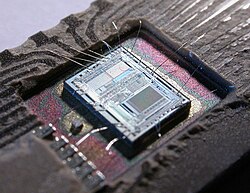
![A Soviet MSI nMOS chip made in 1977, part of a four-chip calculator set designed in 1970[78]](/images/d0/48/d048873dfe57e0392b278a0ce070ecbe7da3ac06e19f1e5fe32a7b3cadfa565a.jpg)
Frequently Asked Questions
ICとマイクロプロセッサは何が違うのですか?
ICは電子回路をひとまとめにした部品の総称であり、タイマーや増幅器など幅広い機能を含みます。一方、マイクロプロセッサはICの一種であり、特にコンピュータのCPU(中央演算処理装置)としての機能を一つのチップに凝縮したものを指します。
なぜシリコンが材料として使われるのですか?
シリコン(ケイ素)は地球上に豊富に存在し、不純物を添加することで電気を通しやすい状態と通しにくい状態を精密に制御できるため、半導体材料として最適だからです。
ムーアの法則とは何ですか?
インテルの共同創業者ゴードン・ムーアが提唱した経験則で、「半導体チップに搭載できるトランジスタの数は、約2年ごとに倍増する」というものです。これは長年、コンピュータの性能向上を予測する指標となってきました。
CMOSとはどのような技術ですか?
Complementary MOS(相補型金属酸化物半導体)の略で、P型とN型のMOSトランジスタを組み合わせて構成される回路です。消費電力が非常に低いため、現代のほとんどのデジタルICに採用されています。
References
- "The basics of microchips". .
- "Integrated circuit (IC)". .
- Wylie, Andrew (2009). "The first monolithic integrated circuits". Archived from the original on 4 May 2018. Retrieved 14 March 2011.
Nowadays when people say 'integrated circuit' they usually mean a monolithic IC, where the entire circuit is constructed in a single piece of silicon.
- ; (1989). The Art of Electronics (2nd ed.). Cambridge University Press. p. 61. .
Integrated circuits, which have largely replaced circuits constructed from discrete transistors, are themselves merely arrays of transistors and other components built from a single chip of semiconductor material.
- Rostky, George. "Micromodules: the ultimate package". EE Times. Archived from the original on 7 January 2010. Retrieved 23 April 2018.
- "The RCA Micromodule". Vintage Computer Chip Collectibles, Memorabilia & Jewelry. Retrieved 23 April 2018.
- Dummer, G. W. A.; Robertson, J. Mackenzie (16 May 2014). American Microelectronics Data Annual 1964–65. Elsevier. pp. 392–397, 405–406. .
- "The Chip That Jack Built Changed the World". Texas Instruments. 9 September 1997. Archived from the original on 18 April 2000.
- US Patent 3138743, Kilby, Jack S., "Miniaturized Electronic Circuits", published 23 June 1964
- Winston, Brian (1998). Media Technology and Society: A History: From the Telegraph to the Internet. Routledge. p. 221. .
📸 フォトギャラリー