私たちが日常的に利用している電子機器から、自然界に起こる落雷まで、電気の挙動は物質が持つ固有の性質によって決まります。その中心となる概念が電気抵抗率(Resistivity)と導電率(Conductivity)です。これらは単なる数値ではなく、物質内部の電子の状態や原子の配列、さらには温度といった環境要因によってダイナミックに変化します。
本記事では、電気の流れやすさを決定づける物理的な定義から、材料ごとの特性、そして温度が与える影響までを詳しく解説します。
Key Facts
- 電気抵抗率 (ρ):電流の流れにくさを表す物質固有の値で、単位はオームメートル (Ω·m) です。
- 導電率 (σ):電流の流れやすさを表し、抵抗率の逆数 (σ = 1/ρ) として定義されます。
- 温度の影響:金属は温度が上がると抵抗が増えますが、半導体は逆に抵抗が減少する傾向があります。
- 極端な状態:超伝導体は抵抗率がゼロになり、絶縁体は極めて高い抵抗率を持ちます。
- プラズマ:電離したガス状態であり、高い導電性を持つ第四の状態です。
電気抵抗率と導電率の基礎定義
物質の電気的な特性を理解するには、まず「抵抗」と「抵抗率」の違いを明確にする必要があります。抵抗 (R) は物体の形状(長さや太さ)に依存しますが、抵抗率 (ρ) は形状に関わらず、その物質自体が持つ固有の性質です。
物理的な計算式
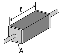
均一な形状の試料において、抵抗率は以下の関係式で表されます。ここで、Rは電気抵抗、ℓは試料の長さ、Aは断面積を指します。
ρ = R × (A / ℓ)
この関係を導き出す基礎となるのが、電界 (E) と電流密度 (J) の比率です。一般的に、ある点における抵抗率は ρ(x) = E(x) / J(x) と定義されます。また、この逆数である導電率 (σ) は、電荷担体(電子や正孔)の密度とその移動度の積に比例します。
テンソルとしての抵抗率
結晶構造などの影響で方向によって電気の流れやすさが異なる場合、抵抗率は単純な数値(スカラー)ではなく、3×3の行列で表されるテンソルとして扱われます。これにより、電界の方向と電流の方向が一致しない複雑な物理現象を数学的に記述することが可能です。
物質による導電メカニズムの違い
なぜ物質によって電気の通りやすさが異なるのか。その答えは、量子力学的なバンド理論にあります。電子が占有できるエネルギー帯(バンド)と、占有できない領域(バンドギャップ)の構成が、物質の分類を決定します。

金属・半導体・絶縁体
- 金属:フェルミ準位がエネルギーバンド内にあり、自由電子が容易に移動できるため、非常に高い導電性を示します。
- 半導体:バンドギャップが存在しますが、熱エネルギーなどによって電子が伝導帯へ励起されるため、条件によって導電性が変化します。
- 絶縁体:バンドギャップが非常に広く、通常の条件下では電子が移動できないため、抵抗率が極めて高くなります。
その他の導電体
固体以外にも、電解質溶液(イオン液体)ではイオンの移動によって電気が運ばれます。また、ガスが電離したプラズマ状態では、自由電子とイオンが混在し、極めて高い導電性を発揮します。例えば、落雷はプラズマによる巨大な放電現象の一例です。
![Lightning is an example of plasma present at Earth's surface. Typically, lightning discharges 30,000 A at up to 100 MV, and emits light, radio waves, and X-rays.[17] Plasma temperatures in lightning might approach 30,000 K (29,700 °C; 53,500 °F), and electron densities may exceed 1024 m−3.](/images/4c/f0/4cf012310643a3dfc125c8d3f683e5a21a2980269d5b4c4b8b488af98ab796c1.jpg)
超伝導現象
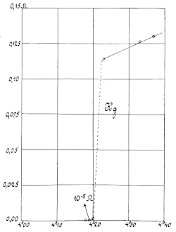
特定の物質を極低温まで冷却すると、ある臨界温度で電気抵抗が突如としてゼロになる超伝導状態に転移します。これは1911年にヘイケ・カメルリング・オンネスによって水銀を用いて発見されました。
温度による抵抗率の変化
ほとんどの物質において、抵抗率は温度 T の関数として変化します。温度変化が小さい範囲では、基準温度 T₀ における抵抗率 ρ₀ と温度係数 α を用いた線形近似式 ρ(T) = ρ₀ [1 + α(T − T₀)] が一般的に利用されます。
材料別の温度特性
金属の場合、温度が上昇すると格子振動(フォノン)による電子の散乱が増えるため、抵抗率が増加します。一方、半導体では温度上昇に伴いキャリア密度が増加するため、抵抗率が指数関数的に減少するという対照的な挙動を示します。
特殊な抵抗挙動
非晶質(アモルファス)半導体では、電荷が局在化したサイト間を飛び移る「可変範囲ホッピング」という現象が見られます。また、近藤絶縁体などの特殊な材料では、フェルミ液体の寄与や近藤効果といった複雑な量子現象が抵抗率に影響を与えます。
主要材料の電気特性まとめ
| 材料区分 | 代表的な物質 | 抵抗率 ρ (Ω·m) | 導電率 σ (S/m) | 特徴 |
|---|---|---|---|---|
| 超伝導体 | 冷却された特定金属 | 0 | ∞ | 電気抵抗が完全に消失 |
| 良導体(金属) | 銀、銅、金 | 10⁻⁸ オーダー | 10⁷ オーダー | 自由電子による高い導電性 |
| 半導体 | シリコン、ゲルマニウム | 可変 | 可変 | 不純物や温度で特性が変化 |
| 電解質 | 海水 | ~2.1 × 10⁻¹ | ~4.8 | イオンの移動による導電 |
| 絶縁体 | ガラス、テフロン | 10¹⁰ 〜 10¹⁶ オーダー | 10⁻¹⁰ 〜 10⁻¹⁶ オーダー | 電子の移動が極めて困難 |
Frequently Asked Questions
抵抗と抵抗率の決定的な違いは何ですか?
抵抗は「その物体(部品)」がどれだけ電流を妨げるかという個別の値であり、長さや太さに依存します。対して抵抗率は「その物質(材料)」が本来持っている性質であり、形状に関わらず一定の値となります。
なぜ金属は温度が上がると電気が流れにくくなるのですか?
温度が上がると、金属内部の原子(結晶格子)の熱振動が激しくなります。これにより、移動しようとする電子が振動する原子に衝突(散乱)する確率が高まるため、結果として抵抗が増加します。
半導体の抵抗率が「可変」であるとはどういう意味ですか?
半導体は、純粋な状態では絶縁に近いですが、少量の不純物を添加(ドーピング)したり、温度を上げたりすることで、導電性を劇的に変化させることができるためです。
超伝導状態になるとどのようなメリットがありますか?
電気抵抗が完全にゼロになるため、エネルギー損失(熱としての放出)なしに電流を流し続けることができます。これにより、超強力な電磁石の作成や、極めて高効率な送電の可能性が開かれます。
プラズマはなぜ導電性を持つのでしょうか?
プラズマ状態では、ガス分子から電子が剥離して自由電子と正イオンに分かれています。この自由な電荷担体が大量に存在するため、ガス状態よりも遥かに高い導電性を示すようになります。
References
- The atomic number is the count of electrons in an atom that is electrically neutral – has no net electric charge.
- Other relevant factors that are specifically not considered are the size of the whole crystal and external factors of the surrounding environment that modify the energy bands, such as imposed electric or magnetic fields.
- The numbers in this column increase or decrease the portion of the resistivity. For example, at 30 °C (303 K), the resistivity of silver is 1.65×10⁻⁸. This is calculated as Δρ = α ΔT ρ0 where ρ0 is the resistivity at 20 °C (in this case) and α is the temperature coefficient.
- The conductivity of metallic silver is not significantly better than metallic copper for most practical purposes – the difference between the two can be easily compensated for by thickening the copper wire by only 3%. However silver is preferred for exposed electrical contact points because corroded silver is a tolerable conductor, but corroded copper is a fairly good insulator, like most corroded metals.
- Copper is widely used in electrical equipment, building wiring, and telecommunication cables.
- Referred to as 100% IACS or International Annealed Copper Standard. The unit for expressing the conductivity of nonmagnetic materials by testing using the method. Generally used for temper and alloy verification of aluminium.
- Despite being less conductive than copper, gold is commonly used in because it does not easily corrode.
- Commonly used for with steel reinforced
- and are considered to replace in fabricated in advanced nodes
- 18% chromium and 8% nickel austenitic stainless steel
📸 フォトギャラリー