Two power MOSFETs in D2PAK surface-mount packages. Operating as switches, each of these components can sustain a blocking voltage of 120 V in the off state, and can conduct a con­ti­nuous current of 30 A in the on state, dissipating up to about 100 W and controlling a load of over 2000 W. A matchstick is pictured for scale.
← ホームへ戻る
MOSFET電界効果トランジスタ半導体CMOSスイッチング

MOSFETの仕組みと進化:現代エレクトロニクスを支えるスイッチング技術

🗓 2026年8月10日

現代のデジタル社会を支えるあらゆる電子機器の心臓部には、MOSFET(金属酸化物半導体電界効果トランジスタ)という極小のスイッチが組み込まれています。このデバイスは、電圧をかけることで電気の流れを制御する能力を持っており、信号の増幅や高速なスイッチングを実現します。スマートフォンからスーパーコンピュータに至るまで、MOSFETなしでは現代のコンピューティングは成立しません。

基本的には、絶縁されたゲート端子に電圧を印加することで、半導体内部の導電性を変化させる仕組みです。これにより、非常に少ない入力電流で大きな負荷電流を制御できるため、従来のバイポーラ接合トランジスタ(BJT)に比べて効率的な動作が可能です。
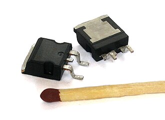
Two power MOSFETs in D2PAK surface-mount packages. Operating as switches, each of these components can sustain a blocking voltage of 120 V in the off state, and can conduct a con­ti­nuous current of 30 A in the on state, dissipating up to about 100 W and controlling a load of over 2000 W. A matchstick is pictured for scale.

Key Facts

  • 基本機能:電圧によって導電性を制御し、スイッチングや信号増幅を行う。
  • 最大の特徴:定常状態においてゲートへの入力電流がほぼゼロであるため、低消費電力である。
  • 主要な種類:キャリアに電子を用いるnMOSと、正孔を用いるpMOSがある。
  • 動作モード:遮断(カットオフ)、線形(オーム)領域、飽和(アクティブ)領域の3つの状態を持つ。
  • 進化の方向:微細化により集積度を高め、処理速度の向上とコスト低減を実現している。

MOSFETの歴史と発展

電界効果トランジスタ(FET)の概念は、1925年に物理学者のジュリアス・エドガー・リリエンフェルドによって提唱されましたが、当時の技術では実用化に至りませんでした。

1957, Diagram of one of the SiO2 transistor devices made by Frosch and Derick[23]

転機となったのは1950年代後半です。ベル研究所のモハメド・アタラとダウォン・カーンが、シリコン表面のパッシベーション(不活性化)と熱酸化技術を応用し、1959年に世界初の動作するMOSFETを開発しました。この発明により、ラジオや計算機、コンピュータの小型化と低コスト化が劇的に加速しました。

構造と動作のメカニズム

MOSFETは、金属(またはポリシリコン)のゲート、酸化膜の絶縁層、そして半導体基板の3層構造(MOS構造)で構成されています。この構造により、ゲートに電圧をかけると電界が発生し、絶縁層の下にある半導体表面に電荷が集まります。
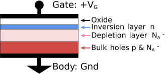
Metal–oxide–semiconductor structure on p-type silicon

例えばnMOSの場合、ゲートに正の電圧を印加すると、p型基板の表面に電子が集まり、ソースとドレインを結ぶ「反転層」と呼ばれる導電チャネルが形成されます。このチャネルを通じて電流が流れるようになります。逆に電圧が低いときはチャネルが存在せず、電流は遮断されます。
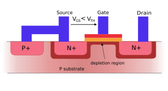
A cross-section through an nMOSFET when the gate voltage VGS is below the threshold for making a conductive channel; there is little or no conduction between the terminals drain and source; the switch is off. When the gate is more positive, it attracts electrons, inducing an n-type conductive channel in the substrate below the oxide (yellow), which allows electrons to flow between the n-doped terminals; the switch is on.

このチャネル形成のプロセスは、エネルギーバンドの曲がりとして説明されます。ゲート電圧によって伝導帯のエネルギーレベルが下がり、電子が充填されることで導電性が生まれます。
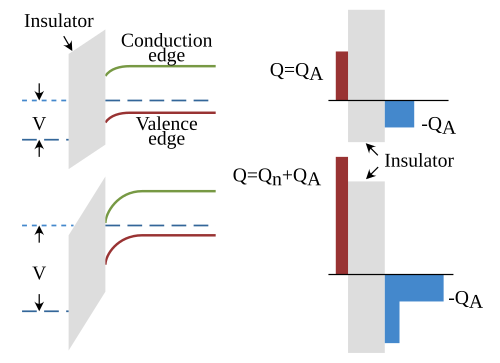
Channel formation in nMOS MOSFET shown as band diagram: Top panels: An applied gate voltage bends bands, depleting holes from surface (left). The charge inducing the bending is balanced by a layer of negative acceptor-ion charge (right). Bottom panel: A larger applied voltage further depletes holes but conduction band lowers enough in energy to populate a conducting channel.

また、チャネルの形成状態は容量-電圧(C-V)特性によっても分析でき、蓄積、空乏、反転という3つの状態を経て動作します。
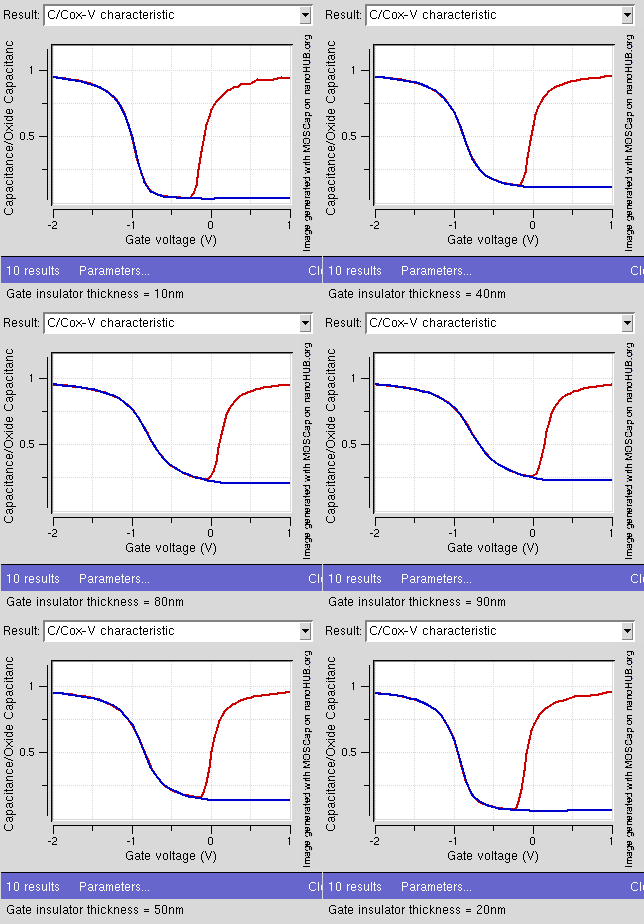
C–V profile for a bulk MOSFET with different oxide thickness. The leftmost part of the curve corresponds to accumulation. The valley in the middle corresponds to depletion. The curve on the right corresponds to inversion.

nMOSとpMOSの比較

MOSFETには、キャリアの種類によってnMOSとpMOSの2種類が存在します。これらは特性が対照的であり、組み合わせて使用することで効率的な回路を構成できます。

nMOS FETとpMOS FETの特性比較
パラメータ nMOS FET pMOS FET
ソース/ドレイン型 n型 p型
チャネル型 n型 p型
基板(ウェル)型 p型 n型
しきい値電圧 (Vth) 正(エンハンスメント型) 負(エンハンスメント型)
反転層キャリア 電子 正孔

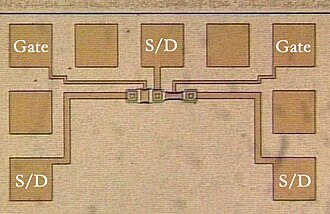
Photomicrograph of two metal-gate MOSFETs in a test pattern. Probe pads for two gates and three source/drain nodes are labeled.

動作モードの詳細

エンハンスメントモードのnMOSを例にとると、動作は主に3つの領域に分けられます。

1. 遮断・サブスレッショルド領域

ゲート電圧(VGS)がしきい値電圧(Vth)を下回っている状態です。基本的には電流が流れませんが、微小なサブスレッショルド電流が流れることがあり、低電力設計において重要視されます。
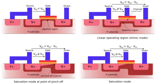
Source tied to the body to ensure no body bias:top left: Subthreshold, top right: Ohmic mode, bottom left: Active mode at onset of pinch-off, bottom right: Active mode well into pinch-off – channel length modulation evident

2. 線形領域(オーム領域)

VGSがVthを超え、ドレイン-ソース間電圧(VDS)が低い状態です。このとき、デバイスは可変抵抗のように振る舞い、VDSに比例して電流が増加します。
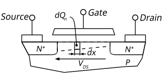
Cross section of a MOSFET operating in the linear (ohmic) region; strong inversion region present even near drain.

3. 飽和領域(アクティブ領域)

VDSがさらに上昇すると、ドレイン付近でチャネルが絞り込まれる「ピンチオフ」現象が発生します。これにより、VDSを上げても電流がほぼ一定となり、増幅器として利用可能な状態になります。

Cross section of a MOSFET operating in the saturation (active) region; channel exhibits channel pinching near drain.

これらの動作特性は、ドレイン電流(ID)とVDSの関係を示す特性曲線によって定義されます。
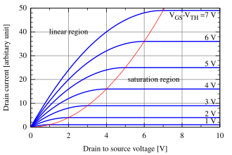
MOSFET drain current vs. drain-to-source voltage for several values of V GS − V th {\displaystyle V_{\text{GS}}-V_{\text{th}}} ; the boundary between linear (ohmic) and saturation (active) modes is indicated by the upward curving parabola.

応用と高度な設計

MOSFETの最大の応用例がCMOS(相補型MOS)回路です。nMOSとpMOSを組み合わせて構成することで、スイッチング時以外に電力をほとんど消費しない極めて低消費電力なデジタル回路を実現しています。
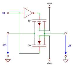
The CMOS analog switch passes the signal through both a pMOS (QP) and an nMOS (QN). When ST is high, the switch provides a low resistance between UA and UB, either of which could be considered the input or output.

また、大電力を扱うパワーMOSFETでは、数千個のセルを並列に配置した構造が採用されており、高い耐圧と大電流への対応を可能にしています。
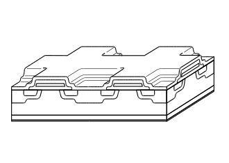
Cross section of a power MOSFET, with square cells. A typical transistor is constituted of several thousand cells.

さらに、アナログ回路ではカレントミラーなどの精密な電流制御に利用され、フィードバック回路を用いて出力抵抗を高める設計が行われています。
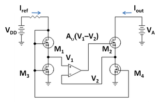
MOSFET version of gain-boosted current mirror; M1 and M2 are in active mode, while M3 and M4 are in ohmic mode, and act like resistors. The operational amplifier provides feedback that maintains a high output resistance.

ボディ効果と寄生ダイオード

ソースと基板(ボディ)の間に電位差がある場合、しきい値電圧が変動する「ボディ効果」が発生します。これは回路設計上の制約となります。
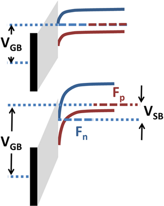
Band diagram showing body effect. VSB splits Fermi levels Fn for electrons and Fp for holes, requiring larger VGB to populate the conduction band in an nMOS MOSFET.

また、構造上、ボディとドレイン・ソース間にp-n接合が生じるため、寄生ダイオードが存在します。これはDC-DCコンバータなどの特定の用途で利用されることがあります。

A 4-terminal nMOS has two intrinsic body diodes due to the body-to-drain and body-to-source p–n junctions. In pMOS, these diodes are reversed. The body-to-source diode is made irrelevant by shorting the body to the source in 3-terminal devices. The remaining body-to-drain diode prevents the nMOS from blocking source-to-drain current and is used in some DC-to-DC converters.[54]

微細化の追求と今後の課題

半導体業界では、チップあたりのトランジスタ数を増やすことで性能を向上させ、コストを下げる「ムーアの法則」に従い、微細化が進んできました。
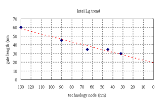
Trend of Intel CPU transistor gate length

しかし、サイズを極限まで小さくすると、ゲート酸化膜からの漏れ電流(リーク電流)の増加や、しきい値電圧の変動(Vthロールオフ)といった物理的な限界に直面します。これを解決するために、ゲート構造を立体的にしたFinFETなどの新しい構造が導入されました。
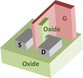
A FinFET

最新のデバイスでは、接合部の浅い設計やハローインプラントなどの高度な製造プロセスが導入され、短チャネル効果の抑制が図られています。
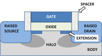
MOSFET showing shallow junction extensions, raised source and drain and halo implant. Raised source and drain are separated from gate by oxide spacers.

ナノワイヤMOSFETのような次世代デバイスでは、さらに精密なチャネル制御が可能になり、しきい値電圧の最適化が進んでいます。
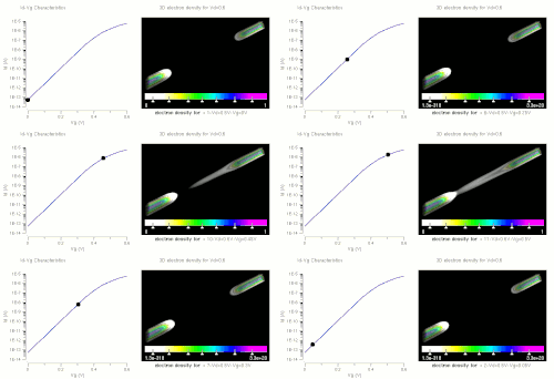
Simulation of formation of inversion channel (electron density) and attainment of threshold voltage (IV) in a nanowire MOSFET. Note: Threshold voltage for this device lies around 0.45 V.

また、LEDなどの負荷を制御するシンプルなスイッチとしても、MOSFETは非常に有効に機能します。

When the switch is closed, the n-channel MOSFET's gate raises above its threshold voltage, so the MOSFET then will conduct current to light the LED.[34]

Frequently Asked Questions

MOSFETとBJTの最大の違いは何ですか?

最大の違いは制御方式です。BJTはベース電流によってコレクタ電流を制御する「電流制御デバイス」ですが、MOSFETはゲート電圧によってドレイン電流を制御する「電圧制御デバイス」です。そのため、MOSFETは定常状態で入力電流をほとんど必要とせず、消費電力が低いという利点があります。

エンハンスメントモードとデプレッションモードの違いは?

エンハンスメントモードは、通常状態でチャネルがなく、ゲートに電圧をかけることで初めて導電性が生まれるタイプです。一方、デプレッションモードは通常状態でチャネルが存在し、ゲートに電圧をかけることで導電性を低下させるタイプです。

CMOSとは具体的にどのような仕組みですか?

CMOS(Complementary MOS)は、nMOSとpMOSを相補的に組み合わせた回路構成です。一方がONのときにもう一方がOFFになるように設計されているため、信号が切り替わる瞬間以外は電流がほとんど流れず、電力消費を極限まで抑えることができます。

微細化が進むとどのような問題が発生しますか?

デバイスが小さくなると、絶縁膜が薄くなるためゲートからのリーク電流が増加します。また、ドレインの電界がソース側に影響を及ぼす「ドレイン誘起障壁低下(DIBL)」などの現象が起き、しきい値電圧の制御が困難になるという課題があります。

FinFETとはどのような構造ですか?

FinFETは、チャネルを魚のひれ(Fin)のように立体的に突き出させ、その三方をゲートで囲む構造です。これにより、平面構造よりも強力にチャネルを制御でき、漏れ電流の削減と動作速度の向上を実現しています。

References

  1. Note: The other enhancement-mode diagrams use a dashed-line along the channel to distinguish it as an enhancement-mode device. However, this particular shorthand above uses a plain line for enhancement-mode and instead uses a thick line to indicate a depletion-mode device.

📸 フォトギャラリー

Two power MOSFETs in D2PAK surface-mount packages. Operating as switches, each of these components can sustain a blocking voltage of 120 V in the off state, and can conduct a con­ti­nuous current of 30 A in the on state, dissipating up to about 100 W and controlling a load of over 2000 W. A matchstick is pictured for scale.
A cross-section through an nMOSFET when the gate voltage VGS is below the threshold for making a conductive channel; there is little or no conduction between the terminals drain and source; the switch is off. When the gate is more positive, it attracts electrons, inducing an n-type conductive channel in the substrate below the oxide (yellow), which allows electrons to flow between the n-doped terminals; the switch is on.
1957, Diagram of one of the SiO2 transistor devices made by Frosch and Derick[23]
Simulation of formation of inversion channel (electron density) and attainment of threshold voltage (IV) in a nanowire MOSFET. Note: Threshold voltage for this device lies around 0.45 V.
Photomicrograph of two metal-gate MOSFETs in a test pattern. Probe pads for two gates and three source/drain nodes are labeled.
Metal–oxide–semiconductor structure on p-type silicon
Channel formation in nMOS MOSFET shown as band diagram: Top panels: An applied gate voltage bends bands, depleting holes from surface (left). The charge inducing the bending is balanced by a layer of negative acceptor-ion charge (right). Bottom panel: A larger applied voltage further depletes holes but conduction band lowers enough in energy to populate a conducting channel.
C–V profile for a bulk MOSFET with different oxide thickness. The leftmost part of the curve corresponds to accumulation. The valley in the middle corresponds to depletion. The curve on the right corresponds to inversion.
Source tied to the body to ensure no body bias:top left: Subthreshold, top right: Ohmic mode, bottom left: Active mode at onset of pinch-off, bottom right: Active mode well into pinch-off – channel length modulation evident
When the switch is closed, the n-channel MOSFET's gate raises above its threshold voltage, so the MOSFET then will conduct current to light the LED.[34]
MOSFET drain current vs. drain-to-source voltage for several values of V GS − V th {\displaystyle V_{\text{GS}}-V_{\text{th}}} ; the boundary between linear (ohmic) and saturation (active) modes is indicated by the upward curving parabola.
Cross section of a MOSFET operating in the linear (ohmic) region; strong inversion region present even near drain.
Cross section of a MOSFET operating in the saturation (active) region; channel exhibits channel pinching near drain.
Band diagram showing body effect. VSB splits Fermi levels Fn for electrons and Fp for holes, requiring larger VGB to populate the conduction band in an nMOS MOSFET.
A 4-terminal nMOS has two intrinsic body diodes due to the body-to-drain and body-to-source p–n junctions. In pMOS, these diodes are reversed. The body-to-source diode is made irrelevant by shorting the body to the source in 3-terminal devices. The remaining body-to-drain diode prevents the nMOS from blocking source-to-drain current and is used in some DC-to-DC converters.[54]
The CMOS analog switch passes the signal through both a pMOS (QP) and an nMOS (QN). When ST is high, the switch provides a low resistance between UA and UB, either of which could be considered the input or output.
MOSFET showing shallow junction extensions, raised source and drain and halo implant. Raised source and drain are separated from gate by oxide spacers.
Trend of Intel CPU transistor gate length
MOSFET version of gain-boosted current mirror; M1 and M2 are in active mode, while M3 and M4 are in ohmic mode, and act like resistors. The operational amplifier provides feedback that maintains a high output resistance.
A FinFET
Cross section of a power MOSFET, with square cells. A typical transistor is constituted of several thousand cells.